ナノインデンターとは(ヤング率測定)

IBIS ナノインデンターとは?

ナノインデンターの測定によって、正確な荷重変位曲線が得られます。
軟かい材料・硬い材料・ラフネス層の工学的に成膜プロセスで作成された、薄膜の特性評価に使用されます。
成膜プロセスには、微小量材料の機械特性の定量測定による熱溶射皮膜も含まれます。


ナノデンターアプリケーションとして、薄膜フィルム・多層金属・ケミカル材料・バイオテクノロジー材料のアプリケーションです。
ポリマー・粘弾性材料・MEMSのフィクスチャーテスト・サブマイクロメートルオーダーの機械特性も評価可能です。

ナノインデンターでは硬度・弾性率・降伏強度・粘弾性(貯蔵損失弾性率)・破壊靭性・耐摩耗性・耐傷性の材料特性も評価可能になります。
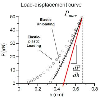
荷重変位曲線荷重変位曲線

製品ラインナップ

ナノインデンター IND

The IND nanoindentation tester system of Semilab is designed to provide a controlled load and deformation of the material being tested. The mechanical response of the material is measured via force and displacement sensors. The range of the actuator, force and displacement sensors, is on the micro- and nanoscale with resolution of nanonewtons and nanometers. The precise nature of the measurement enables us events on the micro- to nanoscale to be recorded. Macroscale damage can thus be interpreted and explained by events on the submicron scale thus allowing the fundamental properties of the sample to be studied and tailored for specific applications.

The force sensor of IND system tools is completely separate from the load actuator and measures the force applied to the indenter directly. Force and depth sensors are independently calibrated against international standards. Closed loop feedback can be selected either for the force or for the depth sensor. Open loop mode of operation for high speed data acquisition is also possible to select. The IND system is almost immune to mechanical breakage due to a specially designed safety gap between the shaft and piezo actuator. Nanoindenter systems use rugged LVDT sensors for both force and depth measurements. Advanced AC amplification provides mV noise floor. Special circuitry offsets the signal to take advantage of the full range of analog to digital converter.

お問い合わせ

ご質問・ご相談はこちら

TEL 045-620-7960

お問い合わせフォーム

日本セミラボ株式会社

〒222-0033
神奈川県横浜市港北区新横浜2-15-10
YS新横浜ビル6階
TEL: 045-620-7960(代表)
FAX: 045-476-2146

セミラボグループ